
Source: Science Advances, doi: 10.1126/sciadv.aay0815
News • Thin film X-ray detector prototype
Revolutionary medical imaging with minimal health risks
Hsinhan Tsai and a research team in materials, nanotechnology, nuclear engineering and X-ray science at the Los Alamos National Laboratory and the Argonne National Laboratory in the U.S. demonstrated a new thin film X-ray detector prototype. The set up contained highly crystalline two-dimensional (2-D) Ruddlesden-Popper (RP) phase layered perovskites and maintained a high diode resistivity of 1012 Ohm.cm, leading to a high X-ray detecting sensitivity of up to 0.276 C Gyair−1 cm−3. To promise revolutionary medical imaging with minimal health risks.
The team collected the signals using the built-in potential and the results underpin the operation of existing robust primary photocurrent devices. The detectors generated substantial X-ray photon-induced open-circuit voltages as an alternate detecting mechanism. The work suggests a new generation of X-ray detectors based on low-cost, layered perovskite thin films for future X-ray imaging technologies.
Solid state radiation detectors can directly convert X-ray signals (radiation photons) into electrical current or charges, with superior sensitivity and a high count rate. The devices can outperform other detection techniques in use to meet critical needs in medical and security applications and in Advanced Photon Source facilities. In order to determine the device detectivity or sensitivity and resolve above the dark noise in a high-performance X-ray detector, scientists must minimize the dark current amplitude at reverse bias and resolve the current generated at low X-ray dosage.
The process requires high purity semiconductors and fully depleted junctions across active regions, while semiconducting materials used for detection also need be robust. Researchers presently use high-purity semiconducting single crystals operating under high voltages across active regions to meet these requirements. Such detectors, however, need a high operational voltage across a large thickness (~ 1 cm), which cause technical challenges such as charge drifting or high fabrication costs to maintain large volumes of monocrystals in scalable imaging applications.
A new type of thin-film device
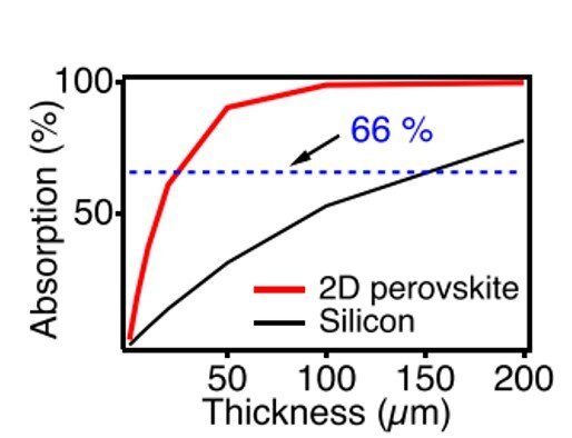
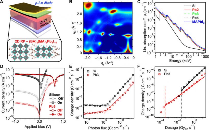
In this work, Tsai et al. designed a new type of thin-film device made in p-i-n junction configuration (three differently doped regions sandwiched between the p- and n- doped region) using 2-D perovskite to efficiently detect X-ray photons. Using synchrotron grazing incidence … gle X-ray scattering (GIWAXS) measurements, the team confirmed superior crystallinity and the preferred orientation in the 2-D thin film. To test the feasibility of perovskite as a radiation detector, they calculated the linear X-ray absorption coefficient (µ1) as a function of incident energy for three different materials, where the values for the perovskite materials were 10- to 40-fold higher than that of silicon. The team explored the strong X-ray absorption observed at perovskite materials, to achieve charge transport and collection across two electrodes. The dark current density for the 2-D RP (Ruddlesden-Popper) device indicated a high dark resistivity of 1012 Ohm.cm as a result of the pin junction and the efficient dark current blocking layers in its constitution. When they exposed the devices to an X-ray source, the team observed a giant increase in X-ray induced current density (Jx) at zero bias (short circuit). Similarly, the 2-D device features also contributed to a larger open-circuit voltage of 650 mV under X-ray exposure at short circuit, compared to a silicon diode (~250 mV).
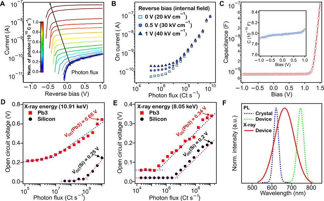
To understand the performance of the superior detector, Tsai et al. examined the power- and field- dependent J-V (current density) characteristics of the device in depth. When they plotted the J-V curves under various X-ray photon fluxes, the device signals decreased with diminishing photon flux. Further observations suggested near-ideal charge collection efficiency under X-ray exposure due to thin-film pin junction design. The results showed the efficiency of the thin-film detector even at low dosage exposure. The high open-circuit voltage (VOC = 650 mV) generated in the device due to the high carrier density further indicated its use as an alternative detection parameter, when VOC scaled linearly with the photon flux during experiments.
The team subsequently measured the X-ray luminescence spectra of the perovskite thin film by probing its visible emission signal under X-ray excitation. The ionized charge recombination pathway helped gain deeper insight into the operational mechanism of the detector. Based on the observations, Tsai et al. noted that when high-energy X-ray excited the material, the charges avalanched and ionized at much higher energy. The charges then transported through states of high and low energy for their eventual collection, yielding an electrical signal. The processes allowed high X-ray induced electrical current signal and high VOC generation without thermal loss to demonstrate the outstanding performance in X-ray detection in the study.
Large built-in field

Another advantage of the thin-film 2-D device architecture included a large built-in field, which facilitated the fast extraction of X-ray carriers. The team stabilized the performance of the device for 30 cycles of voltage scans and X-ray exposures and showed stability of the thin film under both bias and X-ray exposure. In this way, Hsinhan Tsai and colleagues developed a high-quality layered perovskite thin film to engineer a promising candidate to detect radiation. The thin-film device design allowed high sensitivity with an improved detection limit. The device operated with low external bias for stable detection of both low-energy X-ray and ions, with potential applications broadly in medicine and space science.
More information:
Hsinhan Tsai et al. A sensitive and robust thin-film X-ray detector using 2-D layered perovskite diodes, Science Advances (2020). DOI: 10.1126/sciadv.aay0815
B. Durie et al. High speed scintillation autoradiography, Science (2006). DOI: 10.1126/science.1188385
Hsinhan Tsai et al. High-efficiency two-dimensional Ruddlesden–Popper perovskite solar cells, Nature (2016). DOI: 10.1038/nature18306
Source: Science X Network
20.04.2020