
Credit: Sanaz Habibi
News • With less blood splatter
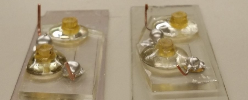
How to make a lab-on-a-chip clear and biocompatible
Lab-on-a-chip devices harness electrical signals to measure glucose, discern blood type and detect viruses or cancer. But biological samples need hafnium oxide for protection from electric fields.
Microfluidic devices can take standard medical lab procedures and condense each down to a microchip that balances on top of a water bottle lid. A team from Michigan Technological University, studying chemical engineering, electrical engineering and materials science, streamline the design of microfluidic devices to be see-through to observe their inner workings. Using hair-thin tunnels and equally tiny electrodes, these devices funnel fluids through an electric current to sort cells, find diseases and run diagnostic tests.
The problem is that biological samples are not inert—they're charged and ready to interact. When fluids come in contact with microdevice electrodes, explosions can happen. Tiny ones. But exploding red blood cells—caused by an ion imbalance that bursts cell membranes in a process called lysis—defeat the point of testing blood sugar levels or blood type. In other tests, like those for cancer or infectious disease, messing with the sample chemistry can lead to faIse negatives or false positives. Interactions between samples and electrodes, called Faradaic reactions, can be an unwanted side effect in microfluidics.
To preserve the integrity of samples and maintain a clear surface to observe what's going on inside the device, Michigan Tech engineers detail how thin hafnium oxide layers act like a cell phone screen protector for microdevices.
Designing a lab-on-a-chip
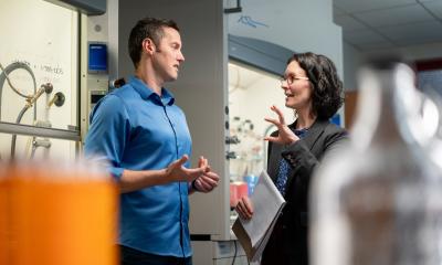
Jeana Collins, lecturer of chemical engineering, studied microfluidics for her doctoral research at Michigan Tech and is the first author on the paper. She explains how the lab-on-a-chip uses a process called dielectrophoresis. "The dielectrophoretic response is a movement," she says. "And how can you tell it moved? By watching it move."
Collins goes on to explain that a non-uniform electric field from the electrodes interacts with the charge on the particles or cells in a sample, causing them to migrate. Many biological lab-on-a-chip devices rely on this kind of electrical response. "As chemical engineers, we deal more with the fluidics side," Collins says, adding that the electronics are also key and a blood glucose meter is a prime example. "You've got the blood—that's your fluid—and it goes in, you have a test done, then you get a digital readout. So it's a combination of fluidics and electronics."
Even though a commercialized lab-on-a-chip like a glucose meter is covered, Collins and other engineers need to see what's going on to get a clear picture under a microscope. That's why hafnium oxide, which leaves only a slight hue, is useful in their microdevice design development.
Also, the technology does not apply to a single device. Because of its simplicity, the hafnium oxide layer works with a number of electrode designs, maintains a consistent dielectric constant of 20.32 and is hemocompatible—that is, it minimizes the Faradaic reactions that can cause cell lysis so fewer red bloods cells explode when they come near the electrodes.
Collins and her team tested three different thicknesses of hafnium oxide—58 nanometers, 127 nanometers and 239 nanometers. They found that depending on the deposition time—6.5 minutes, 13 minutes and 20 minutes—the grain size and structure can be tweaked for the needs of specific devices. The only potential issue would be for fluorescence-based microdevices because the hafnium oxide does interfere with certain wavelengths. However, the layer's optical transparency makes it a good solution for many biological lab-on-a-chip tests.
Clear, Biocompatible and Interdisciplinary
Collins points out that the project's success is directly tied to the team's complementary skills. By bringing together chemical engineers, electrical engineers, materials scientists and the Michigan Tech Microfabrication Shared User Facility, they were able to push the boundaries of all their fields.
"Microdevice design has tended toward increasing levels of complexity; each level of complexity increases probability of failure," says Adrienne Minerick, dean of the School of Technology, professor of chemical engineering and Collins' doctoral adviser. "Simple solutions—while challenging to find—can provide robust, failure-resistant solutions for a wide range of applications. We explored numerous polymeric and inorganic films.”
Source: Michigan Tech
11.10.2018